- 您现在的位置:买卖IC网 > Sheet目录511 > SI5905BDC-T1-GE3 (Vishay Siliconix)MOSFET DUAL P-CH D-S 8V 1206-8
�� ��
��
��Si5905BDC�
�Vishay� Siliconix�
�Dual� P-Channel� 8� V� (D-S)� MOSFET�
�PRODUCT� SUMMARY�
�FEATURES�
�V� DS� (V)�
�-8�
�R� DS(on)� (� Ω� )�
�0.080� at� V� GS� =� -� 4.5� V�
�0.117� at� V� GS� =� -� 2.5� V�
�I� D� (A)�
�-� 4� a�
�-� 4� a�
�Q� g� (Typ.)�
�4� nC�
�?� Halogen-free� According� to� IEC� 61249-2-21�
�Definition�
�?� TrenchFET� ?� Power� MOSFETs�
�?� Compliant� to� RoHS� Directive� 2002/95/EC�
�0.170� at� V� GS� =� -� 1.8� V�
�-� 3.5�
�APPLICATIONS�
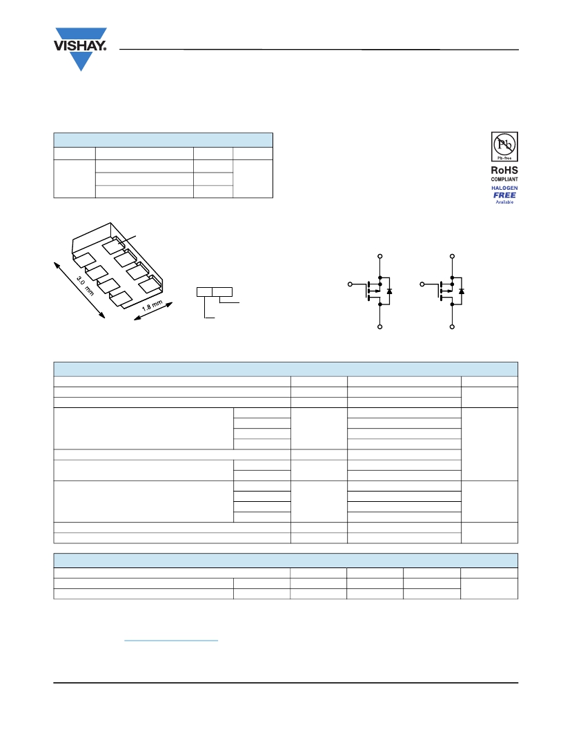
�1206-8� ChipFET� (Dual)�
�?�
�1�
�?� Load� Switch� for� Portable� Devices�
�D� 1�
�D� 1�
�S� 1�
�G� 1�
�S� 2�
�S� 1�
�S� 2�
�D� 2�
�D� 2�
�G� 2�
�Marking� Code�
�DH� XXX�
�Lot� Traceability�
�G� 1�
�G� 2�
�and� Date� Code�
�Part� #�
�Bottom� View�
�Code�
�Ordering� Information:� Si5905BDC-T1-E3� (Lead� (Pb)-free)�
�Si5905BDC-T1-GE3� (Lead� (Pb)-free� and� Halogen-free)�
�D� 1�
�P-Channel� MOSFET�
�D� 2�
�P-Channel� MOSFET�
�ABSOLUTE� MAXIMUM� RATINGS� T� A� =� 25� °C,� unless� otherwise� noted�
�Parameter�
�Drain-Source� Voltage�
�Gate-Source� Voltage�
�T� C� =� 25� °C�
�Symbol�
�V� DS�
�V� GS�
�Limit�
�-8�
�±8�
�-� 4� a�
�Unit�
�V�
�Continuous� Drain� Current� (T� J� =� 150� °C)�
�Pulsed� Drain� Current�
�Continuous� Source-Drain� Diode� Current�
�T� C� =� 70� °C�
�T� A� =� 25� °C�
�T� A� =� 70� °C�
�T� C� =� 25� °C�
�T� A� =� 25� °C�
�T� C� =� 25� °C�
�I� D�
�I� DM�
�I� S�
�-� 4� a�
�-� 3.5� b,� c�
�-� 2.8� b,� c�
�-� 10�
�-� 2.6�
�-� 1.2� b,� c�
�3.1�
�A�
�Maximum� Power� Dissipation�
�T� C� =� 70� °C�
�T� A� =� 25� °C�
�P� D�
�2�
�1.5� b,� c�
�W�
�T� A� =� 70� °C�
�0.94� b,� c�
�Operating� Junction� and� Storage� Temperature� Range�
�Soldering� Recommendations� (Peak� Temperature)� d,� e�
�T� J� ,� T� stg�
�-� 55� to� 150�
�260�
�°C�
�THERMAL� RESISTANCE� RATINGS�
�Parameter�
�Symbol� Typical� Maximum� Unit�
�Maximum� Junction-to-Ambient� b,� f� t� ≤� 5s� R� thJA�
�Maximum� Junction-to-Foot� (Drain)� Steady� State� R� thJF�
�70� 85�
�33� 40�
�°C/W�
�Notes:�
�a.� Package� limited.�
�b.� Surface� mounted� on� 1"� x� 1"� FR4� board.�
�c.� t� =� 5� s.�
�d.� See� Solder� Profile� (� www.vishay.com/ppg?73257� ).� The� 1206-8� ChipFET� is� a� leadless� package.� The� end� of� the� lead� terminal� is� exposed� copper�
�(not� plated)� as� a� result� of� the� singulation� process� in� manufacturing.� A� solder� fillet� at� the� exposed� copper� tip� cannot� be� guaranteed� and� is� not�
�required� to� ensure� adequate� bottom� side� solder� interconnection.�
�e.� Rework� Conditions:� manual� soldering� with� a� soldering� iron� is� not� recommended� for� leadless� components.�
�f.� Maximum� under� Steady� State� conditions� is� 120� °C/W.�
�Document� Number:� 74650�
�S10-0547-Rev.� B,� 08-Mar-10�
�www.vishay.com�
�1�
�发布紧急采购,3分钟左右您将得到回复。
相关PDF资料
SI5915BDC-T1-GE3
MOSFET P-CH 8V CHIPFET 1206-8
SI5915DC-T1-GE3
MOSFET 2P-CH 8V 3.4A 1206-8
SI5933CDC-T1-E3
MOSFET P-CH 20V 1206-8
SI5933DC-T1-GE3
MOSFET DUAL P-CH 20V 2.7A 1206-8
SI5935DC-T1-GE3
MOSFET DUAL P-CH 20V 1206-8
SI5943DU-T1-GE3
MOSFET DUAL P-CH 12V 6A 8PWRPAK
SI5975DC-T1-GE3
MOSFET 2P-CH 12V 3.1A CHIPFET
SI5980DU-T1-GE3
MOSFET N-CH 100V PPAK CHIPFET
相关代理商/技术参数
SI5905DC
制造商:VISHAY 制造商全称:Vishay Siliconix 功能描述:Dual P-Channel 1.8-V (G-S) MOSFET
SI5905DC-T1
功能描述:MOSFET 8V 4.1A 2.1W RoHS:否 制造商:STMicroelectronics 晶体管极性:N-Channel 汲极/源极击穿电压:650 V 闸/源击穿电压:25 V 漏极连续电流:130 A 电阻汲极/源极 RDS(导通):0.014 Ohms 配置:Single 最大工作温度: 安装风格:Through Hole 封装 / 箱体:Max247 封装:Tube
SI5905DC-T1-E3
功能描述:MOSFET 8V 4.1A 2.1W RoHS:否 制造商:STMicroelectronics 晶体管极性:N-Channel 汲极/源极击穿电压:650 V 闸/源击穿电压:25 V 漏极连续电流:130 A 电阻汲极/源极 RDS(导通):0.014 Ohms 配置:Single 最大工作温度: 安装风格:Through Hole 封装 / 箱体:Max247 封装:Tube
SI5905DC-T1-GE3
功能描述:MOSFET DUAL P-CH G-S 8V 1206-8 RoHS:是 类别:分离式半导体产品 >> FET - 阵列 系列:TrenchFET® 产品目录绘图:8-SOIC Mosfet Package 标准包装:1 系列:- FET 型:2 个 N 沟道(双) FET 特点:逻辑电平门 漏极至源极电压(Vdss):60V 电流 - 连续漏极(Id) @ 25° C:3A 开态Rds(最大)@ Id, Vgs @ 25° C:75 毫欧 @ 4.6A,10V Id 时的 Vgs(th)(最大):3V @ 250µA 闸电荷(Qg) @ Vgs:20nC @ 10V 输入电容 (Ciss) @ Vds:- 功率 - 最大:1.4W 安装类型:表面贴装 封装/外壳:PowerPAK? SO-8 供应商设备封装:PowerPAK? SO-8 包装:Digi-Reel® 产品目录页面:1664 (CN2011-ZH PDF) 其它名称:SI7948DP-T1-GE3DKR
SI5906DU
制造商:VISHAY 制造商全称:Vishay Siliconix 功能描述:Dual N-Channel 30-V (D-S) MOSFET
SI5906DU-T1-GE3
功能描述:MOSFET 30V 6.0A 10.4W 31mohm @ 10V RoHS:否 制造商:STMicroelectronics 晶体管极性:N-Channel 汲极/源极击穿电压:650 V 闸/源击穿电压:25 V 漏极连续电流:130 A 电阻汲极/源极 RDS(导通):0.014 Ohms 配置:Single 最大工作温度: 安装风格:Through Hole 封装 / 箱体:Max247 封装:Tube
SI5908DC
制造商:VISHAY 制造商全称:Vishay Siliconix 功能描述:N-Channel 20-V (D-S) MOSFET
SI5908DC_06
制造商:VISHAY 制造商全称:Vishay Siliconix 功能描述:N-Channel 20-V (D-S) MOSFET